Photonic chips represent a fundamental shift in semiconductor technology, using light instead of electrons to process and transmit information. While they will not completely replace electronic chips, they are already transforming specific industries such as telecommunications, data centres, and the automotive sector. This technology offers significant advantages in speed and power efficiency, although manufacturing complexity and cost challenges currently limit broader adoption.
What are photonic chips and how do they differ from electronic chips?
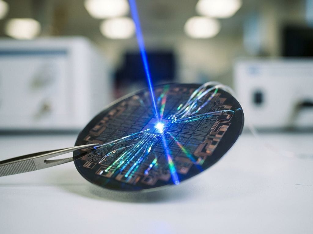
Photonic chips, also known as photonic integrated circuits (PICs), use photons (light particles) to transmit and process data instead of the electrons used in traditional electronic chips. These devices integrate multiple optical components such as lasers, waveguides, modulators, and detectors onto a single substrate, enabling light-based communication and processing.
The fundamental difference lies in their operating principles. Electronic chips rely on electrical current flowing through transistors and conductors, whereas photonic chips manipulate light signals through optical waveguides and components. This creates distinct advantages for specific applications, particularly those requiring high-speed data transmission or optical sensing capabilities.
Three main platforms dominate photonic chip technology:
- Indium phosphide (InP) – Enables direct light generation with excellent properties for advanced signal modulation, making all PIC components manufacturable consistently
- Silicon nitride (SiN) – Offers low-propagation-loss waveguides with the ability to process visible and near-infrared light, benefiting from abundant silicon availability
- Silicon photonics (SiPh) – Provides higher mechanical strength, allowing for large wafer sizes with high yield, and is compatible with existing CMOS manufacturing processes
Each platform serves different applications, with InP excelling in telecommunications and active components, while SiN and SiPh platforms focus more on passive optical functions and integration with existing semiconductor manufacturing.
Where are photonic chips already replacing electronic chips today?
Photonic chips are actively displacing electronic solutions in high-speed data transmission applications, particularly in data centres, telecommunications infrastructure, and automotive LiDAR systems. These applications leverage photonics’ superior bandwidth capabilities and reduced power consumption compared with traditional electronic alternatives.
In data centres and telecommunications, photonic chips power high-speed optical transceivers that handle the massive data demands of modern internet infrastructure. These systems require the exceptional bandwidth that only light-based transmission can provide efficiently at scale.
The automotive sector represents another significant area of adoption, where photonic chips enable fully integrated optical LiDAR solutions essential for autonomous driving systems. These chips provide the precise distance measurement and environmental mapping capabilities required for safe autonomous vehicle operation.
Additional current applications include:
- High-speed networking equipment for enterprise and carrier networks
- Medical sensing devices requiring precise optical measurements
- Industrial sensing applications where electromagnetic immunity is crucial
- Quantum computing systems that rely on photonic components for quantum information processing
The integrated photonics value chain now includes more than 20 specialist suppliers developing components across multiple industries, from healthcare and medical diagnostics to food and agriculture, demonstrating the technology’s expanding real-world implementation.
What advantages do photonic chips offer over traditional electronic chips?
Photonic chips deliver superior data transmission speeds with significantly lower power consumption and reduced heat generation compared with electronic alternatives. They are immune to electromagnetic interference and excel in applications requiring optical sensing, quantum computing, and high-bandwidth communications, where electronic solutions face fundamental physical limitations.
The speed advantage stems from light’s inherent properties: photons travel at the speed of light and do not suffer from the resistance issues that limit electronic signals. This enables photonic chips to handle much higher data rates while consuming less power per bit transmitted.
Key performance benefits include:
- Bandwidth superiority – Light-based transmission supports vastly higher data rates than electrical signals
- Power efficiency – Reduced energy consumption per data operation, crucial for large-scale applications
- Heat management – Lower heat generation eliminates many thermal management challenges
- Electromagnetic immunity – Optical signals remain unaffected by electrical interference
- Parallel processing – Multiple wavelengths can carry different data streams simultaneously
For sensing applications, photonic chips enable miniaturised devices with high accuracy and low cost, particularly valuable in point-of-care healthcare platforms and wearable devices that require precise biomarker monitoring in small form factors.
The technology also offers unique advantages in quantum computing applications, where photonic components provide essential capabilities for quantum information processing that electronic alternatives cannot match effectively.
What are the main limitations preventing photonic chips from fully replacing electronic chips?
Manufacturing complexity and higher production costs are the primary barriers limiting photonic chip adoption. Integration challenges with existing electronic systems, limited general computing capabilities, and the need for specialised expertise and infrastructure further constrain the widespread replacement of electronic solutions.
Each photonic platform faces specific manufacturing challenges. Indium phosphide suffers from higher propagation losses and material brittleness that limit wafer sizes, while also being comparatively expensive. Silicon nitride and silicon photonics platforms require external light sources and face integration complexity with active components.
Cost considerations include:
- Complex fabrication processes requiring specialised equipment and expertise
- Limited manufacturing scale compared with mature electronic chip production
- Integration expenses when combining photonic and electronic components
- Design complexity requiring new tools and methodologies
Technical limitations also constrain adoption. Photonic chips excel at specific tasks such as data transmission and optical sensing but cannot perform the general-purpose computing functions that electronic processors handle efficiently. Most applications require hybrid solutions that combine both technologies.
The industry currently faces a skills gap, with limited availability of engineers and technicians trained in integrated photonics design and manufacturing. This shortage of expertise slows development and increases implementation costs across the entire value chain.
Infrastructure requirements for photonic chip manufacturing differ significantly from those of established electronic semiconductor facilities, requiring substantial investment in new production capabilities and supply chains.
Will photonic chips eventually replace all electronic chips in computing?
Photonic chips will not completely replace electronic chips but will increasingly complement them in hybrid solutions that leverage each technology’s strengths. The future points toward coexistence models in which photonic chips handle high-speed data transmission and optical processing, while electronic chips manage general computing tasks and system control functions.
Industry forecasts suggest that the photonic chip market will grow exponentially, with conservative estimates predicting around 300 million units by 2030 and potentially 1 billion by 2040. However, this growth represents expansion into new applications rather than the wholesale replacement of electronic solutions.
The most likely evolution involves:
- Hybrid integration – Combining photonic and electronic components in single modules to optimise performance and cost
- Application-specific adoption – Photonic chips dominating in communications, sensing, and quantum applications
- Complementary roles – Electronic chips maintaining control functions while photonic chips handle data-intensive operations
- Platform integration – Multiple photonic platforms working together to address complex application requirements
Manufacturing trends indicate that successful photonic chip foundries will need capabilities across multiple platforms – InP, SiN, and SiPh – along with advanced packaging and integration technologies. This suggests a future in which specialised facilities serve the integrated photonics value chain rather than replacing existing electronic manufacturing.
The timeline for broader implementation depends on continued cost reduction, manufacturing standardisation, and the development of hybrid integration techniques. Rather than replacement, the industry is moving toward optimised solutions that combine the best aspects of both photonic and electronic technologies to meet specific application requirements efficiently.
As the photonic industry continues to mature, success will increasingly depend on building a comprehensive ecosystem that supports innovation from research through commercial deployment. The development of human capital remains critical, as the industry needs skilled professionals who understand both the technical complexities and market opportunities in integrated photonics. Companies looking to enter this space will benefit from exploring funding opportunities specifically designed for photonic ventures, while established players may find that internationalisation strategies help them access global markets and partnerships. The future belongs to those who can navigate the intricate landscape of photonic chips while building sustainable business models that leverage both technological advantages and market realities.